Chat freely about anything...

User avatar
By eriksl
#82485 Beside the I think very good tips from others: for MOSFETs to be able to switch their maximum current, they need to be switched (on/off off/on) as quick as possible. Anywhere in between will make the fet dissipate heat and possibly destroy it in the end. MOSFETs tend to store quite a bit of charge in their gate and as the gate is fully isolated, the charge will almost not drain by itself. The ESP8266 has push-pull outputs, so it will try to discharge (and charge) the gate of the MOSFET but it won't do it very efficiently. Also, even though the amount of charge stored in the gate is very small, the rate it which it's charged or discharged is very small, this makes currents flow in between 1 and 20 A (which will probably suprise you). This may very well kill the GPIO sooner or later.

I can recommend to ALWAYS use a MOSFET gate driver (e.g. IR4426 or equivalent). It has a couple of advantages as to connecting MOSFETs to GPIO directly:

- 100% sure the output is push/pull (which is required for proper operation)
- the input has a schmitt trigger so the output is always defined to be completely on or completely off, which makes the MOSFET very probably switch faster than on the GPIO directly
- the output driver fets can sink or source up to 20 A without any problem, and do it fast too, which makes the MOSFETs switch faster, which is better for it's health
- in the unlikely occasion one still messes up, only the driver is broken, not the microcontroller
- but, as far as I am concerned, most important: the input will take almost any CMOS-like level signal and it will output either 0V or Vcc, where Vcc can be anything between 5V and 20V. Most MOSFETs need at least 5-8V to competely turn on (which, again, is required not to blow it). Even if you have a "logical level" MOSFET, it will probably not completely turn on at 3.3V, really.
User avatar
By BillM
#82486
Keep high power circuits away from low power sensitive circuits. You have your connectors on one side and the switching devices on the other side. My guess is that you wanted the mosfets to be on a heatsink, therefor you put them on a clear side of the board. I would have found a better way if that was the case.


Yes I did attach an heatsink. I'm going to do one new PCB layout with the logical stuff on one side and the mosfets on the other.

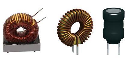
Your circuit requires a lot more current. You can't put resistance in series with the power supply. But you can put inductance in series. Low resistance to DC current, but high impedance to higher frequency waveforms. What you want to do is provide high frequency filtering. Blocking the waveform with the choke and filtering with a capacitor.


Ok, I will do some research on it and how to calculate the inductance value.

Image

We are talking about these inductances like the ones in computer psu, right ?

It provide a low impedance reservoir for the regulator and most regulators need it in order to be stable.


Actually long time ago i've seen someone using it only with capacitor at the output and since I do it this way. But I will add a 22µF if this can help :)

Beside the I think very good tips from others: for MOSFETs to be able to switch their maximum current, they need to be switched (on/off off/on) as quick as possible. Anywhere in between will make the fet dissipate heat and possibly destroy it in the end. MOSFETs tend to store quite a bit of charge in their gate and as the gate is fully isolated, the charge will almost not drain by itself. The ESP8266 has push-pull outputs, so it will try to discharge (and charge) the gate of the MOSFET but it won't do it very efficiently. Also, even though the amount of charge stored in the gate is very small, the rate it which it's charged or discharged is very small, this makes currents flow in between 1 and 20 A (which will probably suprise you). This may very well kill the GPIO sooner or later.


I know that mosfets have inductance effect at the gate so there is high current for a very little time. So the 10k pull-down resistor at the gate might be a problem for high frequency (I mean between 10 and 200Hz) ?
The use of these drivers seems pretty interesting.
I've read the VGS / Id graph of my IRLZ44N and current of +- 25A can flow with 3.3V which is completely fine but you say that if the mosfet is not completely On it will heat ?
So if I give 12V vcc to the driver and I send 3.3V on its input it will power the fet with 12V.

Nice I will try to make a whole new schematic with all the changes and keep you posted.

Thanks for your tips :)
User avatar
By eriksl
#82530 The devil is in the details. You can only check whether a MOSFET is up to the task you require by inspection the SOA (Safe Operating Area). Most (all?) MOSFETs are marketed with ridiculous numbers for current and voltage handling and they're not incorrect in itself, but only in very marginal, not real-life situations and never together ;)

Mentioned in the datasheet is Vth, the voltage at which "typically" the MOSFET starts to conduct. It's always safer to make sure the gate is completely open/saturated. Most MOSFETs can stand up to 14-20 V on the gate and then you know it's fully open ;).

This is all not that relevant for small currents, but if you're switching larger currents, especially if there is an inductance involved, it will make the difference.

You say you added a 10 k pull down resistor to the gate. That will help decharge the gate, but it will not quite help charging it, so it only solves half of the problem. The best approach is the gate driver IC, which will "push" and "pull" the gate forcefully to Vcc and ground.

I am very enthousiastic about those gate driver IC's. I am even using some of them to overcome the capacitance of the single wires of a UTP cable, which in my case is driven bij a 500 kHz signal where the source of the signal isn't low impedance enough to get a nice straight block wave on the line (led pixels). Works like a charm! Kind of a transceiver that way.
User avatar
By BillM
#82627 Alright,

This is what I have done.

Added capacitor to the input of the regulator, maybe a bigger one is needed.
Added a TVS of 15V working voltage to the input, maybe should add to the ouput as well ?
Added a IR4426 mosfet driver
Added 1N4007 Flyback diodes to the outputs
Changed the pcb layout to separate driver side from power side.
Ground is now copper plate in PCB

I did not add an inductor to the input because I don't get the benefits although I think this is the most important change. I'd be happy to ear a great explanation :)

Do you see any other changed I could make to improve this and would it work now if I print new PCB's ? I got to be sure.

Here are my Layout and schematic.

Image

Image

Thank you for helping me !!